 Aleksandr Sidun
Layout-dependent effects (LOD, WPE, Latch-up, Electromigration, Antenna)
1. Latchup
Latch-up is a short circuit/low impedance channel generated between the power and ground rails of a MOSFET circuit, causing IC being inoperable or damaged. It is caused by the formation of the BJT network with a positive feedback.
Latch-Up triggers:
- Power up
- Overshoot voltages and currents
- Substrate noise
- ESD occurrences

Latch-up in CMOS technology (CMOS inverter example)
Let's have a look on a simple circuit example - CMOS inverter. In such a circuit we have one NMOS device formed in a
p-substrate and a PMOS device formed in NWELL. Parasitic NPN device is formed by the n-type source terminal of NMOS,
p-type substrate and n-type NWELL. Parasitic PNP is formed by the p-type source terminal of PMOS, n-type
NWELL and p-type substrate. Of course, both NWELL and p-substrate are lightly-doped meaning that they have some
substantial resistance. Equivalent circuit of a parasitics BJT network is shown on a picture above. Parasitic resistors
and can create a voltage drop during trigger event hereby allowing current flow through BJTs.
This parasitic structure forms a positive feedback, so the current will keep flowing even when trigger is removed,
so the IC has to be powered off to restore normal operation.
Latch-up key points:
- State of an IC when it is made inoperable by a parasitic shorting of VDD and VSS;
- Triggering of a Low Impedance High Current state between supplies;
- High Current State remains even when trigger signal is removed.
As we can see, the main reason for the latch-up is the parasitic resistance of the substrate and NWELL, which allows parasitic BJTs to open during trigger event. As soon as we cannot control the triggers, our primary task would be to reduce the parasitic resistance of the NWELL and substrate. This can be done relatively easily by adding a guard ring of the corresponding type around PMOS and NMOS devices to ensure a strong VDD/VSS potential of the NWELL/substrate and reducing the NWELL/substrate resistance.
Latch-up prevention:
- Guard rings has a lot of contacts, providing a strong VDD/Ground potential;
- Guard rings add more parallel resistance to the NWELL/Substrate, thereby reducing parasitic resistors;
- NWELL/substrate potentials are held around VDD/Ground, no positive feedback is formed.

Latch-up prevention by adding Guard Rings
2. Length of Diffusion (LOD)
Length Of Diffusion effect (LOD) - is the manufacturing effect, which induces stress to the edges of the diffusion area during Shallow Trench Insulation (STI) formation.

LOD effect in CMOS technology
The key steps of the STI process involve etching a pattern of trenches in the silicon, depositing one or more dielectric materials (such as silicon dioxide) to fill the trenches, and removing the excess dielectric using a technique such as chemical-mechanical planarization. These processes include acid and temperature impact on the wafer. STI becomes compressive when the wafer is cooled down, and this leads to the increased holes mobility and decreased electron mobility. Hence, this will improve the performance of the PMOS and degrade the performance of NMOS devices.
LOD key points:
- LOD is the result of the STI formation;
- STI becomes compressive as the wafer cools down;
- The width of STI (active to active spacing) has a strong impact on determining stress;
- LOD improves holes mobility and decreases electron mobility.
LOD effect can be prevented by distancing devices away from the WELL edge (guard ring). This is usually done by placing dummy devices around the circuit devices, in which case your circuit devices will also benefit from the equal edge effects (each device will have the same neighbours).

LOD prevention
3. Well Proximity Effect (WPE)
Well proximity effect (WPE) – is the effect due to lateral non-uniformity in well doping which causes the MOSFET threshold voltages and other electrical characteristics to vary with the distance of the transistor to the well edge.

WPE effect in CMOS technology
The photoresist masks are placed to protect unused areas during N+ or P+ implantation process. During ion implantation process, high-energy ions are bombarding the desired areas, equally distributed across the desired area apart from the edges, where a lot of high-energy ions are reflected from the well photoresist, forming dopants gradient. This difference in dopants concentration will cause a discrepancy between devices, located within the area of the WELL. This may lead to a different speed// etc. of the devices which can be especially critical for the structures like differential pairs and current mirrors.
WPE key points:
- WPE is the result of the N+/P+ area formation;
- WPE introduces dopants gradient;
- Dopants gradient makes devices within WELL unequal;
WPE effect can be prevented by distancing devices away from the WELL edge (guard ring). This is usually done by placing dummy devices around the circuit devices, in which case your circuit devices will also benefit from the equal edge effects (each device will have the same neighbours).

WPE effect prevention by adding dummies
So, in summary:
WPE/LOD prevention:
- Do not place critical devices close to the well edge (guard ring);
- Surround your circuit devices with dummy devices to protect critical devices from LOD/WPE and to ensure similar edge conditions for all devices;

Prevention of LOD and WPE effects
4. Electromigration
4.1 Failure mechanisms
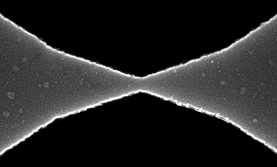
Electromigration - is an electrical effect where electrons on an IC interconnect give some momentum to the atoms that make up the wire. This happens through low energy collisions and subsequent scattering. As a result, the interconnect deforms over time as atoms are moved along the interconnect towards the cathode. This causes pits to appear in the wire closer to the anode, and small metal bumps begin to grow along the surface of the wire closer to the cathode.

Electromigration mechanism
Electromigration key points:
- Occurs at very high current densities (usually >);
- Usually caused by the incorrect wire width for a given current density.
Electromigration process in CMOS technology
4.2 Types of failures
- Void: If the incoming ion flux is lesser than the outgoing ion flux, It will create a void in interconnect. A void can lead a discontinuity in the interconnect and result an open circuit.
- Hillock: If incoming ion flux is greater than the outgoing ion flux, It will cause the accumulation of ions and create a hillock in the interconnect. A hillock can increase the width of a metal interconnect and touch the neighbouring metal interconnect which may result in a short circuit.

Hillocks and voids
4.3 Electromigration prevention
In order to prevent electromigration, designers should strictly follow the manufacturer recommendation for the wire width (because the thickness is specified by the process and cannot be changed) according to the current flowing through the wire. As a sanity check for the layout design, EM/IR analysis can be performed (i.e. using Cadence Voltus tool).
Rule of thumb:
- Calculate width by using vendor-provided formula + 10%;
- Note that the EM is worse at high temperature.
Electromigration prevention techniques:
- Increase the metal width to reduce the current density;
- Use metal stitching (2 or more metal in parallel, connected by vias);
- Reduce the frequency;
- Lower the supply voltage;
- Keep the wire length short;
- Reduce the buffer size in clock lines;
- Avoid path shapes that could lead to inhomogeneous current flow.
5. Antenna effect
The Antenna Effect, also known as Plasma-Induced Damage, occurs when charge accumulates on isolated nodes of an integrated circuit during fabrication, particularly during plasma etching. Plasma's energetic ions and radicals collect on interconnects, increasing their potential. If these interconnects are linked to a transistor gate, accumulated charges may discharge through the thin gate oxide, potentially causing damage or degradation. The risk depends on the surface area of the interconnects—larger areas can lead to higher potentials, increasing the chance of gate oxide breakdown and permanent device damage.

Antenna effect in layout
Antenna Violations prevention:
- Jumper: Long interconnects are rerouted to higher metal layers (metal jumping), typically near the load. This prevents charge discharge through the gate oxide, as higher layers are fabricated later. However, it may increase routing congestion.
- Reduce Via Area: Large via areas can cause antenna violations. Using smaller vias, like converting multi-cut to double-cut or single-cut vias, reduces the cut area but may pose reliability risks such as electromigration.
- Diode Insertion: Placing a diode near the gate on a lower metal layer helps dissipate accumulated charges. The diode, connected in reverse bias (cathode to gate, anode to ground), provides a safe discharge path for static charge.

Antenna effect prevention by using a jumper

Antenna effect prevention by using a diode